Silicon wafer to factory floor
A deep-dive technical guide mapping semiconductor physics directly to active assembly constraints. Learn to model thermal dissipation profiles and optimize active designs for high manufacturing yield.
Standard assembly sequences
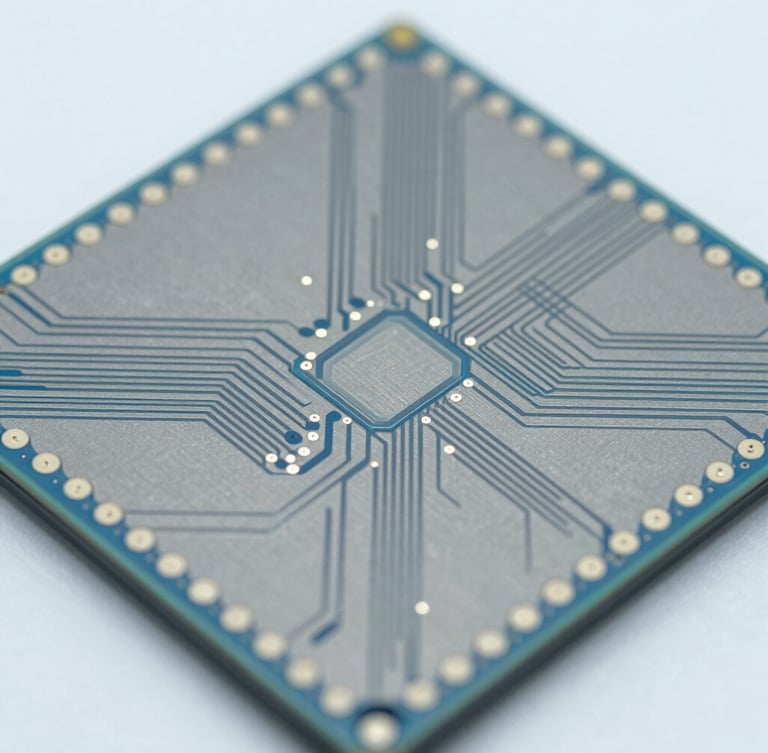
Silicon Die Fabrication
Wire Processing
SMT Assembly Constraints
Photolithography processes define sub-micron transistor geometries on raw silicon wafers, establishing the physical logic layers before packaging. Accurate thermal modeling at this stage prevents active die warping.
Precision drawing and annealing protocols dictate terminal wire tolerances, ensuring low parasitic resistance and consistent signal propagation. We detail micro-coaxial and ribbon wire processing standards.
Surface mount thermal profiles must align with solder paste chemistry to eliminate component shifting and ensure robust mechanical bonds. Reflow temperature curves must be tightly controlled.
Managing physical constraints
High-yield manufacturing demands rigorous alignment between schematic design and factory-floor realities. Engineers must account for thermal dissipation profiles and parasitic capacitance during the initial routing phases to avoid costly re-spins.
Our standardized protocols map tolerance thresholds across diverse assembly lines. By modeling physical assembly limits early, hardware developers systematically reduce defect rates and accelerate production timelines.
Ready to optimize your yield?
Access our complete technical repository of fabrication schematics, tolerance tables, and peer-reviewed assembly papers.