
Electronic Knowledge Technology Engineering
Empowering hardware innovators through direct mapping of raw component physics to active manufacturing process constraints. Access high-fidelity technical schematics and verified semiconductor data.
Verified Physical Specifications
Detailed technical profiles mapping thermal dissipation, tolerance thresholds, and parasitic capacitance across standard hardware categories.
Precision Resistors
Integrated Circuits
Conductor Geometry
Thermal dissipation profiles and tolerance thresholds under active operational loads.
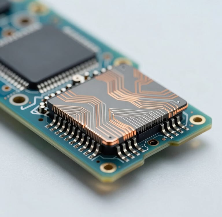
Die-level analysis and parasitic capacitance metrics for high-frequency applications.
Cross-sectional analysis of multi-layer PCB traces and high-spec wiring constraints.
Active Technical Analyses
Recent deep-dive documentation bridging the gap between theoretical semiconductor physics and active factory-floor assembly constraints.
Parasitic Capacitance in ICs
Resistor Heat Signatures
PCB Trace Tolerance
An analysis of die-level proximity effects on signal integrity in high-frequency multi-layer boards.
Mapping thermal dissipation pathways across dense surface-mount arrays to prevent localized board failure.
Correlating manufacturing yield rates with trace width tolerances in high-density interconnect designs.
Access the Engineering Database
Query verified component physical profiles and active manufacturing constraints instantly. Open-access schematics for hardware developers.